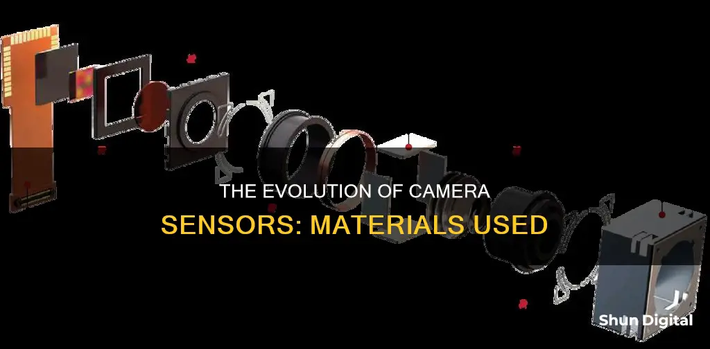
Camera sensors are solid-state electronic devices that can contain millions of discrete photodetector sites called pixels. The two main types of digital image sensors are the charge-coupled device (CCD) and the active-pixel sensor (CMOS sensor). Both CCD and CMOS sensors are based on metal–oxide–semiconductor (MOS) technology, with MOS capacitors being the building blocks of a CCD, and MOSFET amplifiers being the building blocks of a CMOS sensor. Cameras with CMOS sensors tend to be smaller than their CCD counterparts, as digital CCD cameras require additional off-chip ADC circuitry.
| Characteristics | Values |
|---|---|
| Type | Complementary Metal Oxide Semiconductor (CMOS) or Charge-Coupled Device (CCD) |
| Composition | Metal–oxide–semiconductor (MOS) technology |
| Function | Detects and conveys information to form an image |
| Process | Converts light waves into electrical signals |
| Image Formation | Converts electrical signals into colours |
| Components | Millions of cavities called "photosites" |
| Photosites | Open when the shutter opens and close when the exposure is finished |
| Electrical Signal | Varies in strength based on the number of photons captured |
| Colour Images | Requires a filter to determine colours |
| Bayer Filter Array | Consists of alternating rows of red-green and green-blue filters |
| Bayer Array Ratio | One red, one blue, and two green in every section of four photosites |
| Bayer Demosaicing | Translating Bayer array of primary colours into a final image with full colour information at each pixel |
| Microlenses | Enhance light-gathering ability of photosites |
What You'll Learn
![]()
Charge-Coupled Device (CCD)
A Charge-Coupled Device (CCD) is a light-sensitive integrated circuit that captures images by converting photons to electrons. It is made up of millions of cavities called "photosites" that collect photons and store them as electrical signals. Each photosite represents a pixel, and the photons that hit each photosite are interpreted as an electrical signal that varies in strength based on the number of photons captured. This electrical signal is then quantified as a digital value, resulting in a grayscale image.
To capture colour images, a filter, such as the Bayer filter array, is placed over each cavity to allow only particular colours of light to pass through. This enables the camera to determine the colour of an image based on the electrical signals from neighbouring photosites.
CCDs were invented in 1969 at Bell Labs by Willard Boyle and George Smith, who realised that an electric charge could be stored on a tiny MOS capacitor. They are widely used in professional, medical, and scientific applications where high-quality image data is required. While CCDs are still used in some modern cameras, they are being steadily replaced by CMOS sensors due to their lower cost, lower power consumption, and ease of manufacturing.
Materials Used to Make Camera Bags
You may want to see also
![]()
Complementary Metal-Oxide-Semiconductor (CMOS)
CMOS image sensors are made up of millions of tiny light cavities or "photosites" that record an image. When the shutter button is pressed and the exposure begins, each photosite collects photons and stores them as an electrical signal. The camera then measures the strength of the electrical signal to determine how many photons fell into each cavity. This information is then used to create a digital image.
CMOS sensors have several advantages over other types of sensors. They have lower power consumption, higher noise immunity, and can be integrated into a high density of logic functions on a chip. CMOS sensors are also cheaper and have contributed to the development of smaller, more portable electronic devices.
Troubleshooting Guide: Camera Battery Not Charging
You may want to see also
![]()
Bayer filter array
The Bayer filter, named after its inventor, Bryce Bayer, is a microfilter overlay for image sensors that allows photosensors to record light wavelength. The Bayer filter is the most common of such filters and is used in nearly all modern digital cameras. This filter uses a mosaic pattern of two parts green, one part red, and one part blue to interpret the colour information arriving at the sensor. This arrangement is also referred to as RGGB, with the GG representing the proportion of green filter elements and the R and B representing the red and blue filter elements.
Each pixel receives input from all three primary colours, but they are not capable of outputting complete wavelength information since each pixel records only one of the three. Thus, to move from the "Bayer pattern" image to a full-colour image, various algorithms can be used to understand the full-colour values of each pixel. This process is called demosaicing.
The Bayer pattern is a technique that uses an array of colour filters placed over the camera sensor. This limits the requirement for data bits per pixel to a single 8-bit byte. The Bayer pattern is repeated over the image in a fixed configuration to standardise this process. The disadvantage of this approach is that the resolution is reduced; however, most images can be reconstructed using a method of interpolation.
Battery-Powered Wi-Fi Cameras: Night Vision Included?
You may want to see also
![]()
Solid-state sensor
Solid-state image sensors are distinguished by their wide dynamic range, linear response, and high quantum efficiency in the green to near-infrared spectrum. They include charge-coupled devices (CCDs), charge injection devices (CIDs), and addressable photodiode arrays such as Reticon devices. Solid-state image sensors are based on metal–oxide–semiconductor (MOS) technology, with CCDs based on MOS capacitors and CMOS (Complementary Metal Oxide Semiconductor) sensors based on MOSFET (metal-oxide-semiconductor field-effect transistor) amplifiers.
The development of the silicon diode array target for the vidicon was a significant advance in image sensing. The picture charge at each element is discharged through a local switch into a common electrode connected to the output amplifier. The elemental capacitor shunting each diode should be large compared to the stray capacitance shunting the transistor. The elemental capacitor may consist of the depletion layer capacitance between the photodiode and the substrate or the oxide capacitance to an overlying electrode.
Solid-state camera sensors were developed in the 1970s and 1980s, with serious work on solid-state image detectors beginning about 20 years before a significant advance was made with the invention of the CCD. Solid-state sensors have continued to be an area of invention and innovation, with a particular emphasis on conventional television and colour television applications. Infrared solid-state image sensors are an especially active area of research and development.
Blackmagic Pocket Cinema Camera: Powering Your Creative Vision
You may want to see also
![]()
Quantum efficiency
QE varies with different sensor technologies. High-end scientific sensors can achieve a QE of 95%, while photographic film typically has a QE of less than 10%. Charge-coupled devices (CCDs), commonly used in older camera models, can exhibit a QE of over 90% for certain wavelengths. For example, a back-illuminated silicon CCD sensor can achieve a QE of over 90% in the wavelength range of 490-700 nm (visible light). On the other hand, CMOS sensors, which are widely used in modern cameras, may have lower QE values, depending on the specific sensor and wavelength range.
The QE of a camera sensor can be improved through various techniques. For instance, deep-depleted sensors and coated sensors have been developed to enhance QE in the near-red and ultraviolet regions of the visible spectrum, where some sensors exhibit lower QE values. Additionally, the orientation of the sensor within the device can be altered—front-illuminated or back-illuminated—which can impact the QE due to differences in light transmission and attenuation. Back-illuminated sensors, for example, can achieve higher QE values due to reduced attenuation of incident light.
QE plays a significant role in determining the sensitivity of a camera at specific wavelengths of light. However, it is not the sole factor in selecting a camera, and other parameters such as pixel size, read noise, and dark-shot-noise should also be considered when evaluating camera performance. By understanding the QE and its limitations, camera manufacturers can design sensors that optimize light sensitivity and image quality under various lighting conditions.
Understanding Bulb Exposure Mode in Photography
You may want to see also
Frequently asked questions
The two main types of camera sensor are the charge-coupled device (CCD) and the complementary metal-oxide-semiconductor (CMOS).
A CCD sensor is a silicon chip that contains an array of photosensitive sites. The chip moves charge packets around using clock pulses and a shift register, before converting them to a voltage via a capacitor.
A CMOS sensor is a digital device that converts the charge from a photosensitive pixel to a voltage. It also multiplexes the signal by row and column, using on-chip digital-to-analog converters.
CCD sensors are slower but offer higher sensitivity and pixel-to-pixel consistency. CMOS sensors are faster, have lower power consumption, and are smaller in size, but have lower sensitivity and higher noise levels.